Our research approaches
Novel nanoscaled electrical devices rely on the design of tailored architectures. For this purpose nanoparticles are intensively investigated. So far, electrical characterizations concentrated mainly on thin films, but it is still a challenge to establish reliable, high quality assemblies of nanocomponents. We will develop truly two-dimensional continuous materials and two-dimensional monolayer films composed of individual nanocrystals by the comparatively fast, inexpensive, and scalable colloidal synthesis method. The synthesis mechanisms and the materials’ properties will be studied in detail, especially regarding their (photo-) electrical transport. Using these structures we will develop new types of device structures, such as Coulomb blockade and field enhancement based transistors. Recently, we demonstrated the possibility to synthesize, in a controlled manner, truly two-dimensional colloidal nanostructures. We will investigate their formation mechanism, synthesize further materials as “nanosheets”, develop methodologies to tune their geometrical properties, and study the (photo-) electrical properties of individual nanosheets. Furthermore, we will use the Langmuir-Blodgett method to deposit highly ordered monolayers of monodisperse nanoparticles. Such structures show interesting transport properties governed by Coulomb blockade effects known from individual nanoparticles. This leads to semiconductor-like behavior in metal nanoparticle films. The understanding of the electrical transport in such “multi-tunnel devices” is still very limited. Thus, we will investigate this concept in detail and take it to its limits. Beside improvement of quality and exchange of material we will tune the nanoparticles’ size and shape in order to gain a deeper understanding of the electrical properties of supercrystallographic assemblies. Furthermore, we will develop device concepts for diode and transistor structures which take into account the novel properties of the low-dimensional assemblies. Nanosheets and monolayers of nanoparticles truly follow the principle of building devices by the bottom-up approach and allow electrical transport measurements in a 2D regime. Highly ordered nanomaterial systems possess easy and reliable to manipulate electronic properties what makes them interesting for future (inexpensive) electronic devices. Based on our experiences and investigations and with the integrated physico-chemical approach with different expertise we will investigate the electrical transport mechanisms in modern nanoparticle superstructures.
Two-dimensional colloidal nanostructures
In regard to inexpensive, high-perfomance photovoltaic applications we investigate the synthesis and the opto-electrical performance of two-dimensional nanomaterials, such as colloidal lead sulfide nanosheets. We are interested in tuning their geometry (lateral extensions and height). Tuning the height allows the manipulation of their effective bandgap, which means that it will be possible to adapt the bandgap to the requirement of the target application. We characterize the structures as individual items or as thin films.
Electrical transport through thin films of nanoparticles
Different techniques such as Langmuir-Blodgett and spin-coating are used and optimized in order to deposit thin films of monodisperse nanoparticles on electrode structures defined by electron-beam lithography. We can generate mono- or multi-layer films using metallic or semiconducting nanoparticles. In order to characterize such films we perform electrical transport measurements. They usually show nonlinear characteristics depending on the temperature. Such films can be used as chemical sensors or for cheap electronic devices.
Attachment of inorganic nanoparticles to carbon nanotubes
Novel applications in nanotechnology rely on the design of tailored nano-architectures. For this purpose, carbon nanotubes and nanoparticles are intensively investigated. We study the synthesis of inorganic nanoparticles by means of colloidal synthesis and their attachment to carbon nanotubes. We investigate the chemical and electronic properties of such composite structures, since they are potentially interesting for applications in photodetectors, solar cells, and fuel cells.
Electrical transport through individual nanostructures
We synthesize inorganic nanostructures by colloidal synthesis or chemical vapor deposition. For example, needle-shaped nanostructures composed of an In head and an InP tail with lengths up to several micrometers were generated in a one-pot synthesis. Owing to their specific design such In/InP nanoneedles suit the use as ready-made Schottky transistors. Furthermore, we investigate the modification of the electronic properties of carbon nanotube based transistors.
Carbon nanotube electronics
We are investigating the electronic transport in carbon nanotubes field effect transistors and the influence of organic and inorganic adsorbates. On the one hand such adsorbates could be tailored tetrathiafulvalene derivatives which attach to the nanotube in a pincer-like fashion. On the other hand we investigate the charge transfer upon adsorption of inorganic nanoparticles. Those structures are interesting with regard to sensors and solar cells.
Videos about the colloidal synthesis of nanostructures

Bitte beachten Sie: Sobald Sie sich das Video ansehen, werden Informationen darüber an Youtube/Google übermittelt. Weitere Informationen dazu finden Sie unter Google Privacy.
Animation of a setup for the synthesis of colloidal nanoparticles
Bitte beachten Sie: Sobald Sie sich das Video ansehen, werden Informationen darüber an Youtube/Google übermittelt. Weitere Informationen dazu finden Sie unter Google Privacy.
Synthesis of colloidal PbS nanosheets
Bitte beachten Sie: Sobald Sie sich das Video ansehen, werden Informationen darüber an Youtube/Google übermittelt. Weitere Informationen dazu finden Sie unter Google Privacy.
Transformation of energy
Bitte beachten Sie: Sobald Sie sich das Video ansehen, werden Informationen darüber an Youtube/Google übermittelt. Weitere Informationen dazu finden Sie unter Google Privacy.
The Alexander-von-Humboldt Foundation asked Christian Klinke: What does it mean to be a Humboldtian?
Equipment
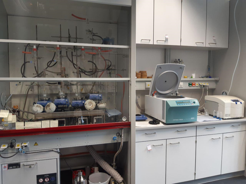
Fully equipped chemistry labs for the synthesis of colloidal nanomaterials.
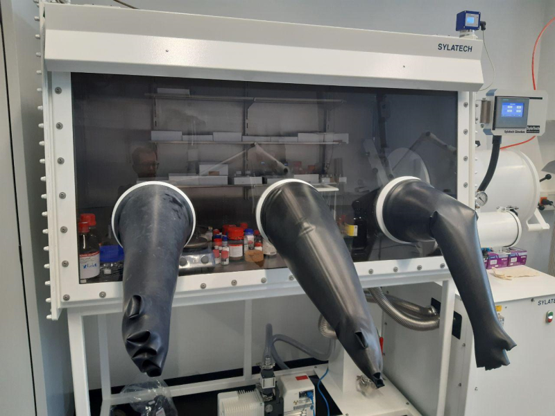
Glove box for the storage and the preparation of oxygen and moisture sensitive chemicals and samples.
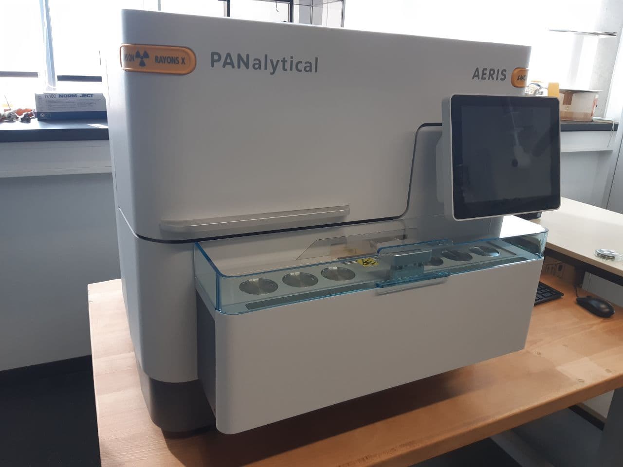
X-ray diffractometer for the crystallographic analysis of solid state samples over a wide angular range. This instrument is funded by the European Regional Development Fund of the European Union.
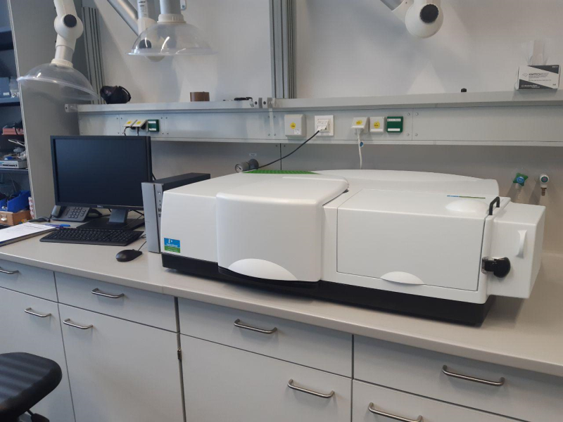
Absorption spectrometer with integration sphere and three detectors for a wide spectral range.
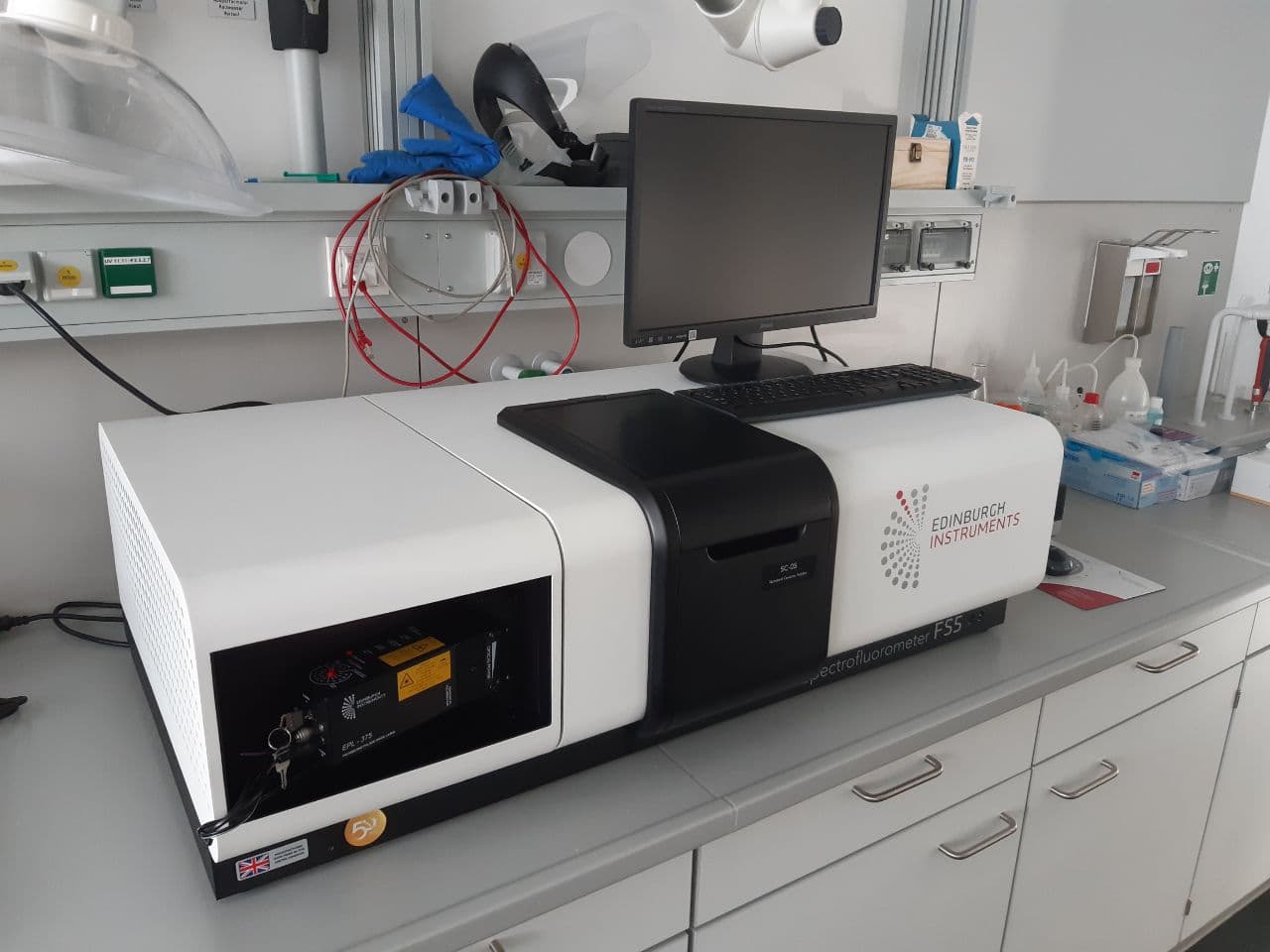
Photoluminescence spectrometer with integration sphere and time-correlated single photon counting. This instrument is funded by the European Regional Development Fund of the European Union.
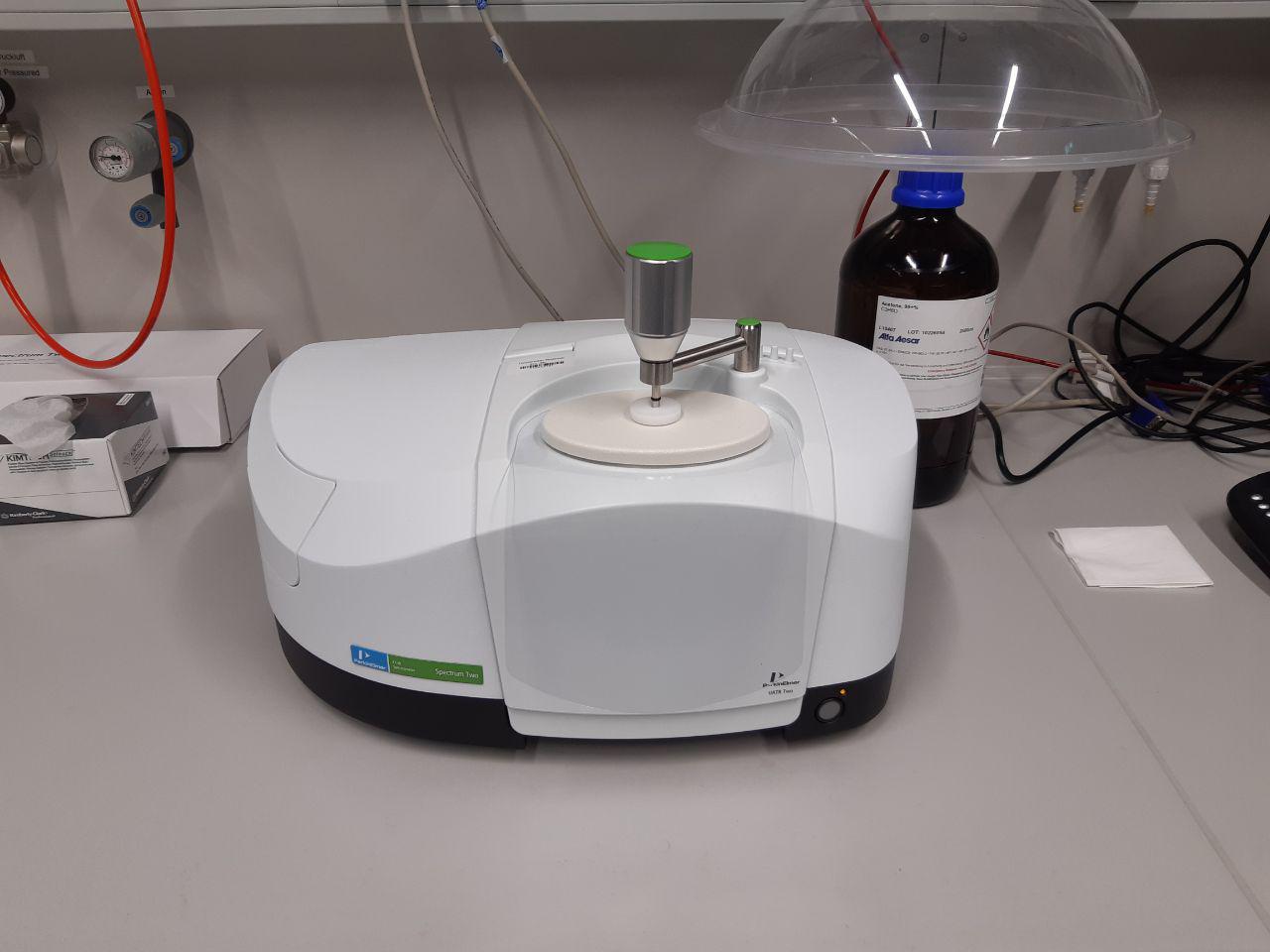
FTIR spectrometer with ATR unit for analyses in the infrared range.
Cryogenic probe stations for optoelectronic transport measurements at low temperatures.
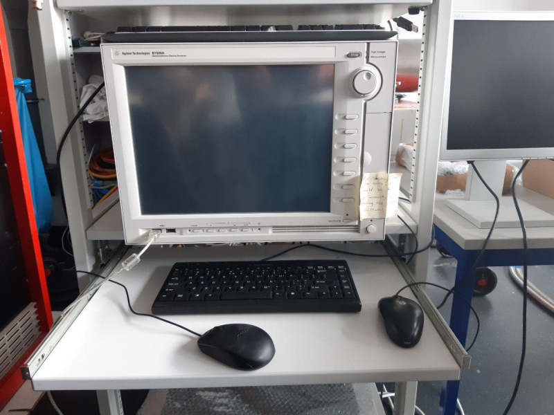
Semiconductor parameter analyzers to measure electrical currents very precisely.
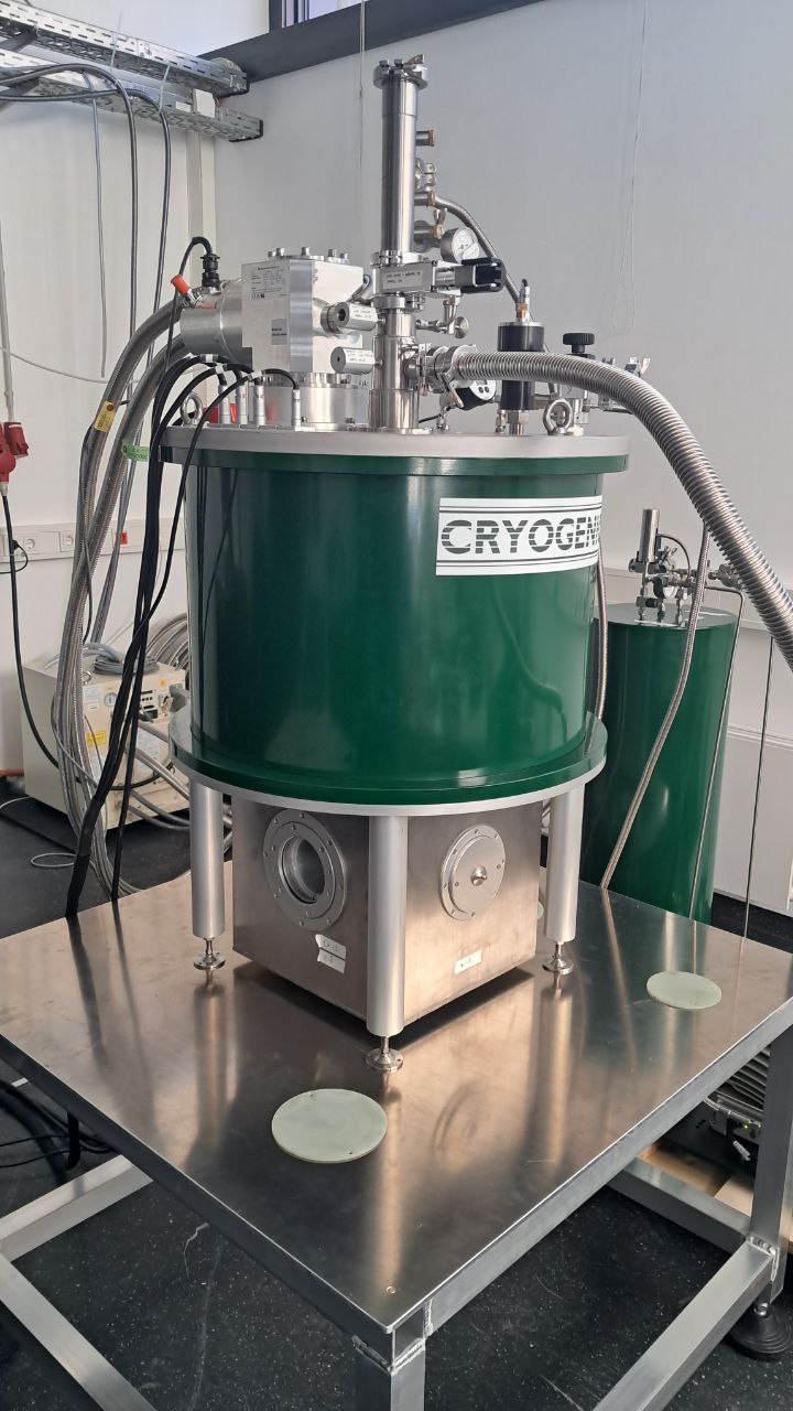
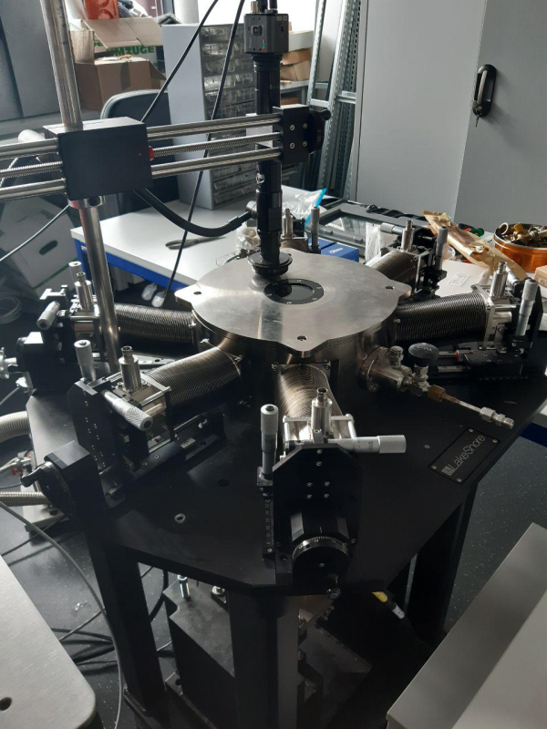
Cryostat (base temperature 1.7 K) with magnetic field (up to 7.5 T) to perform (time-resolved) optical spectroscopy and electrical transport measurements as these conditions.
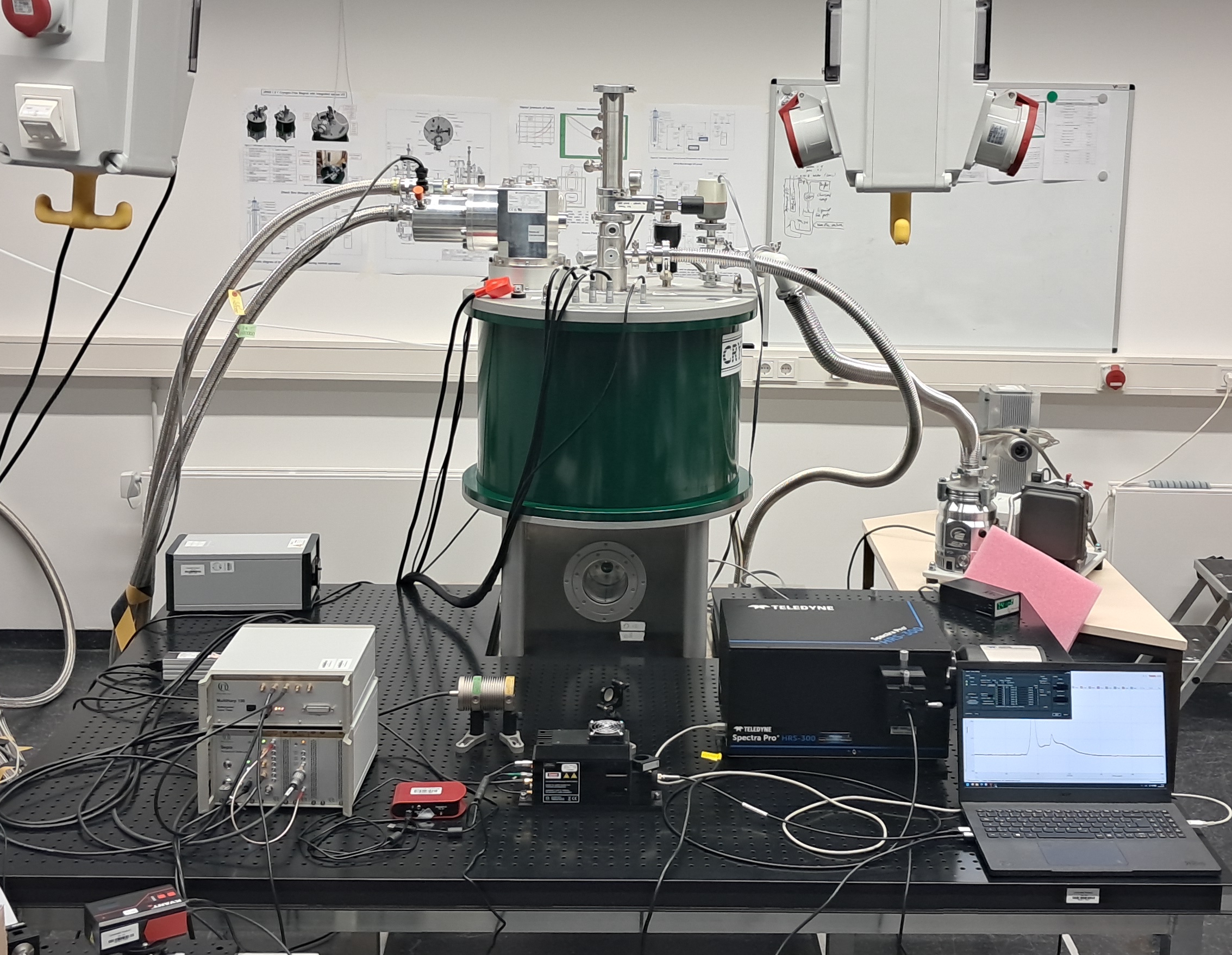
Time-resolved spectroscopy at low temperatures and high magnetic fields allowing for detailed studies on the optical properties of nanostructures. This instrument is funded by the European Regional Development Fund of the European Union.
Simulation computers to support the experimental findings with molecular dynamics and band structure calculations.
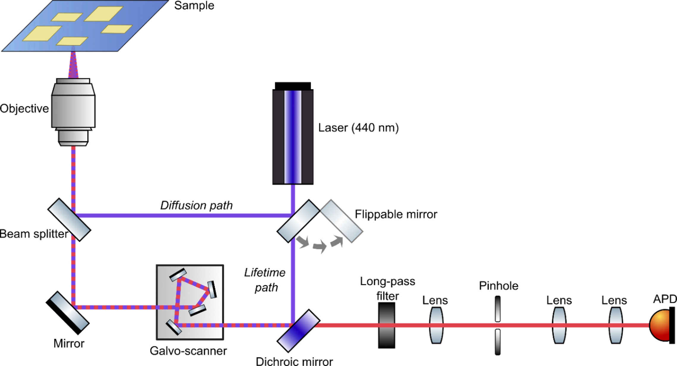
Fluorescence Lifetime Imaging Microscopy FLIM for diffraction limited analysis of optoelectronic charge-carrier relaxation and transport.

Transmission electron microscopy to image the inner and outer structure of nanocrystals. See also: ELMI-MV.